Advanced Electronic Materials (Fujita Lab)
Our fruitful daily life has significantly been indebted to the innovation in semiconductor materials. At the same time we are facing the severe problems of the environment. It is our duty yo out descendant to establish the technological breakthroughs which not only to further enrich our life but also to protect the environmental degradation of our planet.
- We are reluctant to depend on toxic materials such as arsenic and phospholous in semiconductors. Oxide semiconductors, on the other hand, may be developed as environmental friendly and stable device materials.
-
We should be aware of the depletion of rare metals such as indium, nickel, bismuth, and so on, which have widely been used in various devices. We are requested to develop the substitute materials.
-
We are pleased to invite new technologies for semiconductor growth and processing which are safe and friendly to environment and to workers.
It is our goal to develop new semiconductor materials, thin films, organic materials, growth technilogies, and devices which can contribute to the protect and save evironment of our planet.
Academic Staff
Shizuo FUJITA
 Professor (Graduate School of Engineering)
Research Interests
Advanced functional materials, Nano quantum materials
Contacts
Rohm Plaza Rm.305, Katsura Campus
E-mail: fujitasz kuee.kyoto-u.ac.jp
Kentaro KANEKO
Assistant Professor (Graduate School of Engineering)
Research Interests
Contacts
Introduction to R&D Topics
Oxide Semiconductors for Photonics and Electronics
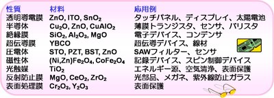
There are numerous kinds of oxide materials. Oxides exhibit variety of functions, for example, superconducting, insulating, magnetism, photo emission, and so on. We pay attention to oxide semiconductors and are aiming at developing photonic, magnetic and electronic functions with the environmental-friendly materials.

Wide Band Gap Semiconductors and Devices with Deep Ultraviolet Optical Functions
Increasing demand for exploring ultraviolet (UV) to deep UV (DUV) optical devices has recently accelerated. UV to DUV detectors are necessary for such as monitoring UV rays in the environment, measuring output power of UV to DUV lamps in the fields of disinfection, the environment as well as UV lamps, and detecting certain genes. UV to DUV emitters are indispensable for high efficient white light sources and future optical disk systems. In addition to the general interests on semiconductor materials such as AlN, AlGaN, ZnMgO, and diamond, our efforts are focused on gallium oxide (Ga2O3). This semiconductor has the direct bandgap of about 4.8eV, that is, the binary material possesses the potential for DUV devices. In addition, the bulk substrates are available and the bandgap engineering is expected alloying with Al and In. As a research group in University, we are eager for pioneering contribution for this quite new material system.
Functionalized Semiconductor Nano Structures
Unique functions are expected in nanometer-sized semiconductor structures, which may successfully contribute to new functional and high performance photonic and electronic devices. We are developing controlled semiconductor nanostructures and investigating their photonic and electronic properties toward device applications.

Environmental Frieldly Technologies for Thin Film Growth
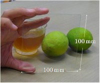
Enormous energy has generally been required for semiconductor growth and processing. High vacuum systems, high temperature processes, toxic sources, complex control/safety systems, and remaining wastes; our comfortable and convenient life has been gained at the huge cost of our planet. Suppose a more environmental friendly growth technology, which is low cost, consumes low energy, and uses safe sources, but is capable of growing superior quality materials and structures. It is not a dream but our need for future earth. Evolution of environmental friendly materials (such as oxide semiconductors) with environmental friendly growth technology; it is our goal.

Photonics and Elctronics of Organic Thin Films and Devices
Chemistry people have great skills in designing, functionalizing, and actually synthesizing organic molecules and materials. Organic materials are basically composed of carbon, hydrogen, and oxygen, and may be categorized as environmental friendly materials. We are especially interested in optical properties of organic material thin films, and our efforts are directing for controlled growth of films and multi-layered structures, analysis of photonic and electronic properties, and applications to novel devices.

