Optoelectronic Materials Science and Engineering (Kawakami Lab)
Our lab is working on discovering and elucidating new material properties based on the interaction between light and materials, as well as developing new optical devices and applications that utilize these properties. Some of the research themes we are pursuing are listed below.
- Development of polychromatic emitting low-level InGaN miniature light source
- Exploration of optoelectronic material properties through measurement of optical dynamics
- Optical biosensing
- Patenting and commercialization/venture startup for white LED goggles
While items (1) to (4) can be viewed as being individual themes, they are all dependent on one another. For example, although the aim of (1) is to use nanostructural control to develop the ultimate optoelectronic material (i.e., a material of any size capable of emitting light of any wavelength with 100% efficiency in any location) this is closely linked with (2), which is indispensable for providing positive feedback on fundamental optoelectronic characteristics in materials development research.
In addition, as an example of application of optoelectronic material properties, we envision the following developments in the field of biomedical applications. We envision in the not-too-distant future the advent of micromachines that are implanted in the human body, as anticipated in the movie "Fantastic Voyage." Such technology would need to incorporate microscopic high-definition solid-state lighting and solid-state imaging devices, and would require optical spectra synthesizers to detect subtle differences in color tone. In addition, by using a combination of fluorescent materials that can selectively capture only lesion sites with solid-state lighting, such technology is expected to result in an extensive range of potential applications for diagnosing and treating cancerous tissue. For this, (1) and (2) are connected with (3) and (4).
While solid-state lighting is obviously useful for general applications such as automobile headlights, it also has much potential to provide micro- and nano-sized light sources. To help make these a reality, we are working with great dedication on fundamental optical science research and materials development and related bio applications.
Academic Staff
Yoichi KAWAKAMI
 Professor (Graduate School of Engineering)
Research Interests
Contacts
TEL: +81-75-383-2310
FAX: +81-75-383-2312
Mitsuru FUNATO
Associate Professor (Graduate School of Engineering)
Research Interests
Contacts
TEL: +81-75-383-2311
FAX: +81-75-383-2312
Ryota ISHII
Assistant Professor (Graduate School of Engineering)
Research Interests
Contacts
TEL: +81-75-383-2311
FAX: +81-75-383-2312
Introduction to R&D Topics
Evaluation techniques for photophysics phenomena
Through our research to date, we have demonstrated that in a nitride semiconductor light-emitting element there is potential fluctuation in the luminescent layer of nanometer proportions, and that this determines the optical characteristics through the activity of the nano-localized center of the carrier.
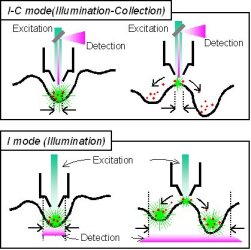
Conventionally, this kind of microscopic-level carrier behavior was observed not by direct observation, but rather by a method combining macroscopic measurements with the construction of a model. In our lab, we are pursuing development work on microscopic optical measurement techniques such as scanning near-field optical microscopes, with the aim of establishing nano-optical sensing techniques that can directly capture such behavior and determine its variation with time.
The figure below shows an outline of carrier dynamics observation based on multimode near-field spectroscopy.

Basic technology for elucidating and enhancing the performance of photophysics phenomena
To understand the way that semiconductor light-emitting elements produce light, it is essential to understand the behavior of the carriers (i.e., electrons and positive holes). In our research, we study and elucidate the behavior of these carriers, which continually varies from moment to moment, using ultra-short pulse lasers—capable of tracking carrier motion with a time resolution of 10–12 to 10–15 seconds—as well as near-field optical microscopes and confocal laser microscopes—capable of tracking motion in the nano to sub-micro range.
Particularly when nano-localized centers contribute to light emission (as is the case with nitride semiconductors), a large number of elementary factors, including carrier excitation, diffusion, mitigation, capture, and recombination affect the optical characteristics that are ultimately observed.Through this kind of research, which correlates carrier dynamics and the characteristics of other elements, we aim to develop elements having superior luminous efficiency.
The figure below shows the emission mapping results of the InGaN quantum well structure observed using a multimode near-field spectrometer. The arrows indicate contrast variations caused by carrier diffusion.

Development of new optical functional materials and devices by nanostructure control
Up until now nitride semiconductor light-emitting devices have used two-dimensional quantum wells. In view of this, our lab is focusing on microstructure to determine how light-emission characteristics could be varied by controlling structure three-dimensionally.
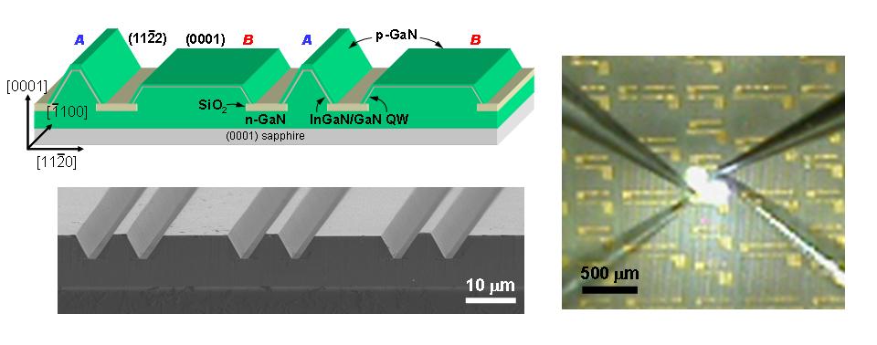
We expect that controlling three-dimensional structure will enable the creation of various new functions and possibilities—such as enhanced luminous efficiency based on artificial control of nano-localized centers, multicolor light emission based on different structural characteristics (e.g., composition and film thickness) for different surfaces, and enhanced luminous efficiency based on polarization reduction in inclined surfaces.We are fabricating these kinds of structures using metal organic chemical vapor deposition, which is now extensively used in industry, and are evaluating their physical properties.
The figure below shows a schematic outline and a scanning electron microscope image of a three-dimensional microstructure, and a white light-emitting element based on such a structure.

Industrial applications of high-performance optical devices
In general, it is necessary to cultivate new applications for developed technologies to ensure that they become widely adopted.
This lab focuses on special-purpose applications of illumination products based on semiconductor light-emitting devices (light-emitting diodes and laser diodes), and proposes potential applications, such as the use of nitride semiconductor white LEDs for medical lamps and for illuminating cultural treasures.
We believe that cultivating these kinds of unexplored fields of application can lead to new industries being spawned.
The photo below shows a prototype of LED goggles.

